Matsushita Super Micro Electro-Discharge machine (MG-ED72W)
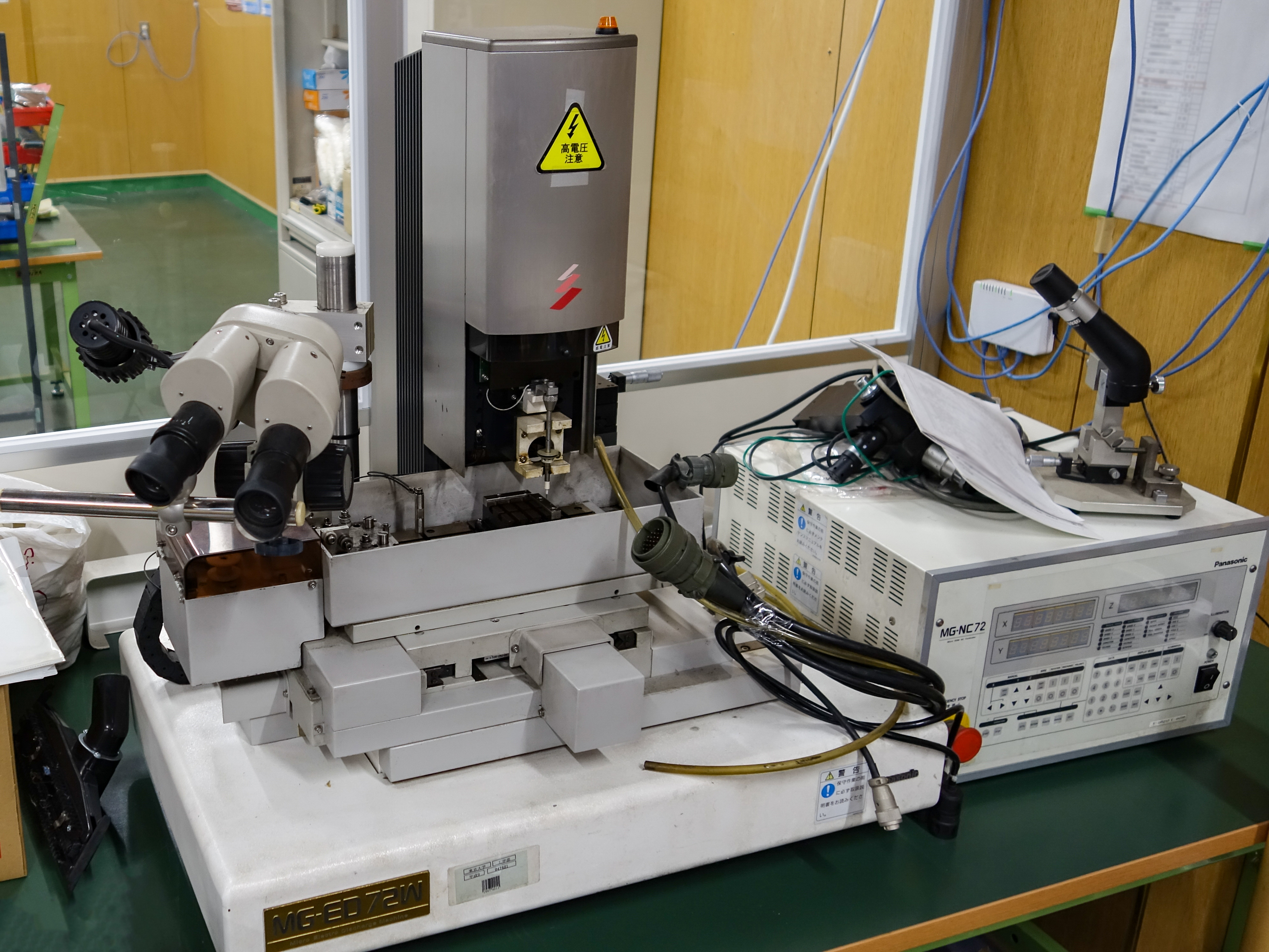
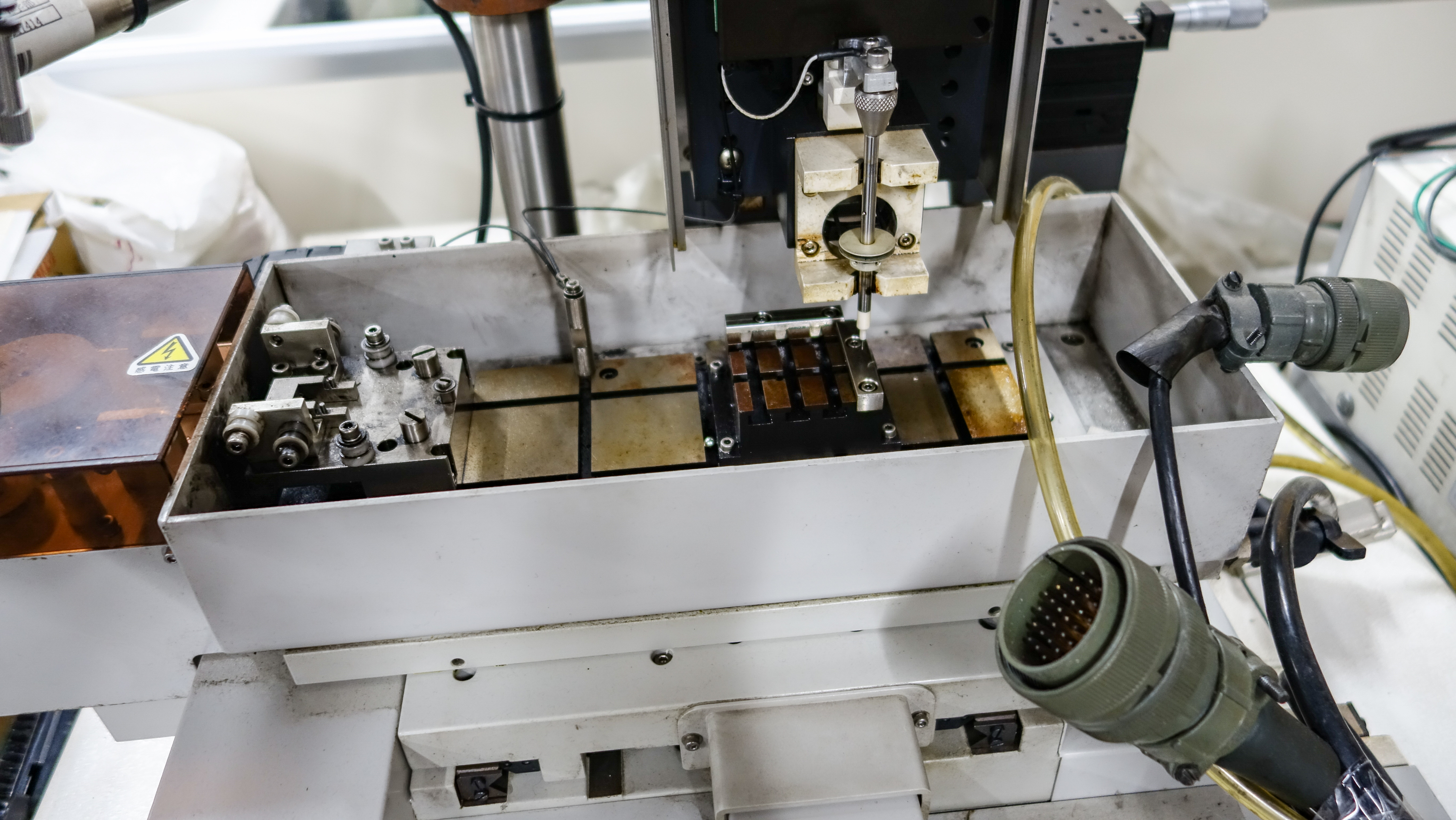
Overview
The processing size is small but it is possible to process high-hardness materials and high-resistivity materials (like silicon). It is also possible to undertake complex three-dimensional processing.Spec.
Processing range: X200mm Y50mmLocation-deciding resolution: 0.1um
Electrode movement distance: 10mm
バナースペース
Global Center in Engineering Education Institute for Innovation in International Engineering Education,
Graduate School of Engineering,
The University of Tokyo
〒113-8656
Building no. 8,
the Faculty of Engineering, 7-3-1 Hongo, Bunkyo-ku, Tokyo
TEL 03-5841-8800